![]() Перевести
эту страницу на русский язык
Перевести
эту страницу на русский язык
My new homebrew oscilloscope: a valuable instrument with few efforts
Introduction
After I have made my first oscilloscope, I used it where I could, and it gave me really plenty of help. Nevertheless, I wanted more: to look at the high-frequency signals in detail in order to tune my HF equipment, to have calibrated and linear X-axe, to have flat frequency response in range at least of several megahertz. All my attempts to modernize my first design were unsuccessful - but what could be expected from that primitive schematics! I probably should thank it, that it worked as it did. When i tried to look in the special literature for the scope's schematics, i found only those, which were not far away from my first one. In that time an idea came into my mind - to repeat some of industrial design. These designs have much improved repeatability compared to those published in amateur's magazines, because they are actually repeated thousand times during manufacturing processes. Also, wide-band techniques were new for me, and to prevent potential disappointment from the difficulties encountered, it was the best choice for me to build valuable instrument with reasonable efforts.
With a kindly help of my friend, I got the schematics of S1-73 model of the scope. This unit was actually used by the person, who gave it to me, and he was completely satisfied with the performance.
I started to make one block after another, and the work went quite well. Everything, that i did, worked as it should (This was an industrial design). None of the designs, described in amateur literature, behaved like this. After everything was finished, i tried to improve what i have done. After some time the final construction had the following parameters:
bandwidth about 25 MHz (in the original - only 5 MHz),
maximal sweep speed - about 50 nanosec/division (the screen is divided onto 10 horizontal divisions and 6 vertical ones; in the original - 100 ns/div),
maximal calibrated sensitivity - 20 mV/div (In the original it was 10 mV/div, but i used another CRT, and due to this fact and also at the expense of the bandwidth the gain has decreased)
Block-schematics of the unit and short description
The oscilloscope consists on the following blocks, which actually are made on the separate printed circuit boards:
Low-voltage power supply, which gives +10V and -10V for the most circuits in the instrument.
Input frequency-compensated attenuator, with four fixed positions: 0, -20,-40 and -60 dBV.
Signal channel wideband amplifier, excluding final stage. It performs the signal amplification from the initial level to several volts.
Final stage of the signal amplifier. Using just four two transistors, it gives up to 200V of signal , required by the CRT.
Synchronization trigger, which forms the synchronization impulses from the monitored signal and enables control over the synchronization process.
Sweep generator, which gives the saw-shaped signal for the sweeping.
X-channel amplifier.
High-voltage power supply with beam blanking trigger. This block gives all necessary voltages (-2000V and some others near it) for CRT feeding as well as +150 and +300V for the feeding of final stages in 'Y' and 'X' channels. Since the beam blanking trigger has very high potential over the ground, it was reasonable to include it into that 'dangerous' block.
Low voltage power supply.
I guess, this is the simplest block in the unit, schematics of which is given below.
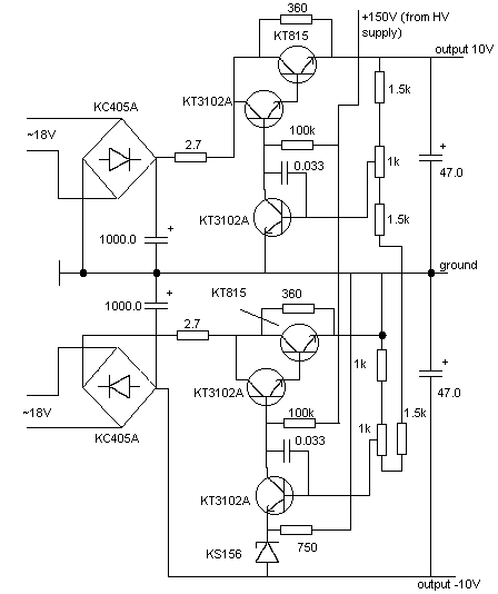
Every channel uses separate winding of the same power transformer and separate diode bridge for AC->DC conversion. The stabilizers have common compensational design. In order to use the same transistors (n-p-n) in '+' and '-' channels, transistor regulator is introduced into the 'hot' wire in '+' channel, and into the 'ground' wire of negative channel. Two pairs of transistors are used as DC amplifiers, and two others - as negative feedback To avoid the influence over the feedback stages, they are fed from the independednt power supply (+150V), located in high-voltage block. The whole schematics seems rather unusual and even strange, and probably the constructors of the original unit were restricted in p-n-p transistors, otherwise i could not explain, why not they used common solutions. Nevertheless, I found this stabilizer quite good for this scope, the output was almost free from industrial frequency (50 Hz) pulsations at the currents consumed. Voltages on outputs are set exactly to +-10V by the semi-variable resistors in appropriate channels.
Input attenuator
Though this block does not contain any active device, it is responsible for one of the most important parameter of the unit - flat frequency response of signal channel in wide range of input signal's values. If the frequency response have significant deviation from the optimal one, signals with complex spectrum (only ideal sinewave have the spectrum, which consists from one component) will be displayed incorrectly, since some components are amplified more, than another ones, spectrum is distorted, and the shape displayed will belong to that 'distorted' signal. For example, if the channel has significant fall down of the frequency response, signals will be 'smoothed', and you probably will see instead of rectangular pulse something like slightly distorted sinewave.
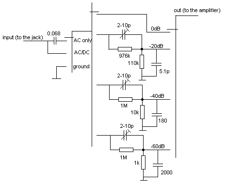
The design actually implemented is completely the same, that i described in another page. There are 3 independent attenuators (for -20, -40 and -60dBV), which are switched by mechanical switch. Special attention should be paid for proper construction. The inputs are well shielded from the outputs, as well as from the rest of schematics. Otherwise, flat frequency response at high attenuations (-40, and especially at -60 dB) will be unachievable due to 'leak' of powerful input signal into high-sensetive input of the amplifier. In my case, the attenuator is made on double-sided small PCB, which is between two plates of mechanical switch (one plate switches input signal to the specified attenuator, the other one connects the channel's input to the attenuator's output). The copper pour serves as the shield, and the whole block is also shielded to prevent undesired couplings and RF leakage. Small variable capacitors (~10pF) are used to set the frequency response of each attenuator to the proper value.
Special tree-position switch is used to switch input modes. In 'AC only' the input signal passes through capacitor, which cuts off the DC components. In 'AC/DC' mode the signal goes to the amplifier as it is, and the 'ground' position is used to examine zero level of the signal channel.
Signal wideband amplifier
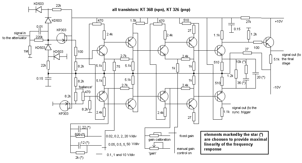
Y-channel amplifier uses differential design technique, as the most of wide band amplifiers for test equipment. The first stage is just a source follower, which provides high input impedance, required for accurate measurements. The gate of the 'upper' (on the schematics) transistor serves as a signal input, the second gate is grounded (its potential is zero). Semi-variable resistor in the drain circuit is used to set balance the initial stage, and, therefore, the whole amplifier.
The subsequent stage is made on four bipolar transistors of different types. The first pair (npn) forms a classical differential stage, and the next one - differential emitter repeater. To decrease the overall gain, provide stable working and flat frequency response, negative feedback is introduced trough 2.7k resistors between emitters on npn transistors and collector of p-n-p ones. In this stage the amplification correction is also performed. It is needed due to the fact, that input attenuator provide only four positions, and for convenient operation it is required much more. By the setpoints 0.1, 1 and 10 Volts/division nothing is switched in parallel with a resistor chain between emitters of n-p-n transistors and the amplification is minimal. If the sensitivity is set to 0.05, 0.5, 5 and 50 V/div, additional RC circuit is introduced. This causes reduction of negative feedback and increase of the total amplification in 2 times. The capacitor in this circuit is chosen to provide flat frequency response. Analogously works another correction circuit, which is used in the positions: 0.02, 0.2, 2 and 20 V/div. Here the amplification is 5 times more, that 'uncorrected' one.
The third stage has almost the same design, as the second one. Here the gain correction also exists and is used to provide manual amplification control. Typically the gain of this stage is fixed and is determined by the 'calibration' semi variable resistor. But if you set the gain control to 'smooth', you can manually stretch the image in vertical dimension by the varying the feedback value in this stage by the corresponding potentiometer.
The fourth stage has a simple two-transitor differential design. Here, the signal amplitude is quite significant, and therefore this stage determines the frequency response of the whole amplifier. To provide maximal linearity, two frequency-dependent circuits (one capacitor and one RC-chain) are introduced between emitters. These capacitors, as well as other correcting capacitors must be carefully chosen to provide maximal linearity of frequency response of the whole signal channel.
From the collector of the 'upper' transistor signal goes through emitter follower to the final amplifier, and from the another output of this stage - to the synchronization trigger.
Sorry for the extreme width of this picture...
The tuning of this block is rather simple. If everything is done well, the amplifier should work properly. The only things to be done are:
balancing of the schematics by the corresponding semi-variable resistor
biasing of stages number 2 and 3. If this is done, in case of shortened input output voltage should not change by the gain switch in the second stage, as well as by the gain change in the third one
setting proper frequency response by varying of the correcting capacitors
calibration of relative gain by varying of the resistors in correcting chains in the second stage
calibration of absolute gain to provide proper vertical display scale
All this stuff should be done only after the whole signal channel is assembled, and this amplifier works in conjunction with the final one and the CRT.
Final stage of the signal amplifier
The schematics of this amplifier is quite straightforward and is completely the same as the last stage of the wideband amplifier.
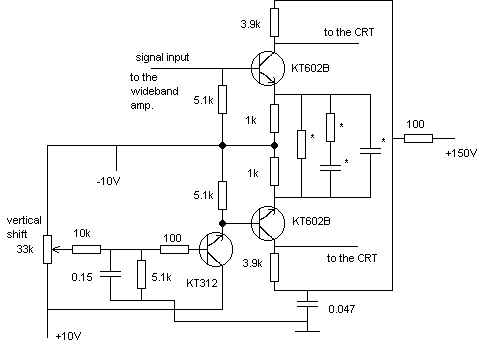 Output transistors are fed by the 150V supply and consume a couple watts
of power and therefore require small heatsinks. The most tricky question
here is selecting of the resistor values in collector and emitter circuits,
as well as correcting capacitors (these components are marked by the star
(*) on the schematics) . If the collector resistors are too big,
the output power is too small and the stage can't feed capacitive loading
(CRT) on high frequency without significant response fall down. Otherwise,
if they are too small, gain decreases, dissipated power increases. To
retain the gain by the collector current increase, resistors in emitter
circuit have to be decreased too, which yields non-linearity and other
bad effects. The goal is to choose the compromise between dissipated
power, linearity, gain and frequency response. Some of the gain loss with
the frequency can be compensated by the capacitors in emitter circuit.
Output transistors are fed by the 150V supply and consume a couple watts
of power and therefore require small heatsinks. The most tricky question
here is selecting of the resistor values in collector and emitter circuits,
as well as correcting capacitors (these components are marked by the star
(*) on the schematics) . If the collector resistors are too big,
the output power is too small and the stage can't feed capacitive loading
(CRT) on high frequency without significant response fall down. Otherwise,
if they are too small, gain decreases, dissipated power increases. To
retain the gain by the collector current increase, resistors in emitter
circuit have to be decreased too, which yields non-linearity and other
bad effects. The goal is to choose the compromise between dissipated
power, linearity, gain and frequency response. Some of the gain loss with
the frequency can be compensated by the capacitors in emitter circuit.
I tried many combinations of parameters, and finally got the passband upto 25 MHz with a reasonable dissipated power. Unfortunately, on the frequencies beyond 12-15 MHz the amplifier can't provide the voltage for full-sized picture (only about 60% of screen's height). The schematics of the final stage is represented on the picture, and I suppose, no additional comments are needed here. I must excuse, that I do not give the precise values of the elements, which determines frequency response here. To find out them, I have to open the unit and look at the actual resistor and capacitor values. I still can not overcome the bad habit not to properly document, what I have done.
Synchronization trigger
This block takes the signal from the output of the wideband signal amplifier and forms from it rectangular impulses, which are further used in sweep generator to control sweeping process. To customize the synchronization according to user's requirements, the polarity of the signal, which the impulse is formed from, may be chosen, as well as the level, which the impulse is formed at.
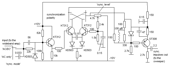
The trigger block has three stages. First one is a emitter follower, which serves as a input buffer stage. The connection between the input and the wideband signal amplifier may be direct ('AC/DC' position of 'synchronization mode' switch) or through a capacitor ('AC only' position of the switch). Practically, there is no significant need in such switch, because the retaining or eliminating of the DC component may be done on the input of the scope, but it is probably useful in some special cases.
Then, the signal goes to one input of the differential stage on two identical transistors. This stage works as a comparator between the input signal and the DC from the wiper of the potentiometer marked 'sync. level'. By this potentiometer, DC voltage on the second input is controlled and therefore, the treshold of the intensity of input signal, which causes the exchange of the potentials at the outputs (collectors), is determined. The 'polarity' switch position determines, from which collector the signal will be taken and processed further (voltages on the collectors are paraphase). Actually, this switch is perfomed in my case by small-sized relay to avoid long wires and, therefore, undesired parasite effects.
After the differential stage the signal becomes the shape of almost rectangular impulses, which rises up every time when the voltage on the input exceeds the sync. level and fall down when the input signal falls down below the sync. level - there is no hysteresis (Note, that words 'up' and 'down' here have only relative sense). These impulses may be directly used for synchronization, but they have not very sharp fronts, and on high frequencies this may cause poor image quality (the sharpness will be insufficient).
To amplify the impulses formed in the second stage and to decrease the duration of the fronts, the third stage is introduced. This has typical common-emitter design, which works in saturation mode. Tunnelling diode in the base circuit serves for further decreasing of signal front's duration. From the collector of the last stage the formed synchronization impulses are going to the sweep generator.
Sweep generator
I guess, this is the most important, but the most complicated block in the whole construction. When I made it, I did not understand completely, who it works. But having done it, I saw, that it worked, and worked pretty good. Even now I would not try to comment the schematics here, because I really do not understand completely, how it works. On the next picture the diagram is presented, excluding frequency-determining circuits (they are attached to the points marked 'A', 'B' and 'C'). The sweep generator has one input used for synchronization and two outputs - one for sweeping itself and one - for the beam blanking during backpath. In the 'external sweep' mode the generator does not work (it is turned off by the 'left' part of the 'sweep mode' switch) and the output of the block is connected to the 'X-input' jack. This design appeared to be quite repeatable, and only two semi-variable resistors are used to adjust the shape of the output signal and to achieve good stability and linearity of the working. It also should be noted, that the first transistor (from sync. input) should be made from germanium, not from silicon. Silicon devices refuse to work here due to higher shift voltages required for them.
According to my expirience, this construction should work if it is done properly. At least, I did not encounter any difficulties. The only tuning required is setting output signal parameters (such as amplitude, stability, linearity, minimal delay between impulses on fast sweeping), setting reset treshold for each sweeping speed band by varying corresponding capacitors in frequency-determining circuits and , of course, calibrating of the sweep speed in the middle position of the 'speed' potentiometer by varying corresponding R and C values. Maximal calibrated speed is 100 ns/div, but the uncalibrated one is about 50 ns/div, which is enough for working with signals with frequencies upto 20-25 MHz.
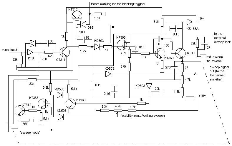
Nevertheless, the presented schematics differs a lithe bit from original one, described in technical data for this model of the scope. The differences are in the organization of frequency switching, because originally a 18-position three-directional switch was required, and I made the schematics only with two three-position switches (one selects the order multiplier - 0.1, 1 and 10, another one selects additional multiplier - 1, 2 or 5) and one additional knob which selects the sweep speed between milliseconds and microseconds scale. The combinations of all values form 18 positions from 50 ms/div to 0.1 microsec/div. The frequency-determining circuits are presented separately, on the next picture.
As you may see, sweep speed is controlled on three levels. On the first one, three resistors are switched, which have resistances in proportion 1 : 2.5 : 5. By this way, common multiplication coefficients 1, 2 and 5 are provided. Changing of the sweep speed in 10 or 100 times is provided by switching appropriate capacitors, which have capacitances in proportions 1:10:100. Except time-determining capacitors (on the right side), additional capacitors (on the laft side) are switched, which provide stable working and proper reset treshold in each subband (their values are chosen to achieve good synchronizability and minimal 'idle time' of the sweeper) . Finally, changing the sweep speed between ms/div and ms/div (in 1000 times) is performed by the special knob, which selects between two groups of capacitors in both sections (by this knob, 4.7 microfarade capacitor is changed to 4.7 nanofarade one etc.). On the fastest sweep the corresponding capacitor is smaller as it could be expected (47 pF) due to the influence of schematic's internal capacity. When practically tuning this block, it is sometimes nessesary to use insted one capacitor two - first main one and the second one - as the 'corrective' in order to achieve nessesary proportion of sweep speeds in different positions.
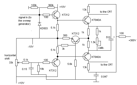
X-channel amplifier
The schematics used in this block is principally the same, as in signal final stage. The gain of X-channel is much lower, that the gain of Y-channel, and only two stages are used between the sweer generator (or the external sweep source) and the CRT. The first stage is a common differentional emitter-repeater, which serves to ensure high input impedance. As in signal final stage, the second input of the differentional amplifier is used change DC component at the output and, by this way, to move the picture in vertical dimension. Final stage is made on high-voltage transistors, which can handle up to 300 volts. The gain of the whole amplifier, determined by the ratio of resistors in collector and emitter circuits in the final stage, is much higher, than in Y-channel and the additional semi-variable resistor is used to adjust the gain for time domain calibration purposes. As usual, higher gain is provided at the expense of the bandwidth, which does not exceed 1-1.5 MHz here.
High-voltage power supply with beam blanking trigger
The principles, implemented in this block, are described on my another page, including simplified graphical representation. As it may be seen, there are four (!) power supplies - one gets 2 kV for anode feeding, another two ones serve for focusing and brightness control (note, that these supplies and associated circuits have potential about 2 kV relative to the ground, which require adequate safety precautions and proper insulation), and the last one - for the blanking trigger. Actually, this block contains one additional combined supply, which gives +150 and +300 V for Y- and X- final amplifiers. Such number of the supplies require adequate number of secondary windings on the power transformer, and I could not find the core, which had enough space to wind so many windings. That is why I used three small transformers - this solution is not really nice from technical viewpoint, though probably the best one for practical homebrewing. The complete circuit diagram is presented below.
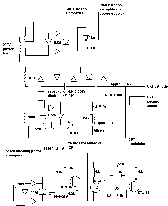
On the top of the schematics you may see the power supply for the final amplifiers. It is made by the simplest schematics possible and gives +150 and +300V for 'Y' and 'X' final stages respectively. Here, secondary winding with the 'middle point' is required, and such transformers are rather rare. I used an old device, which had been used in some tube equipment. Anode (secondary) winding serves as the primary one (!), and the primary, which was made to work from 127 and 220V power lines and has, therefore a 'middle point', serves as the secondary one.
Another secondary winding, which gives about 300 VAC, is attached to the voltage multiplier on 5 diodes and 5 capacitors, which gives at the output about 2 kV. The elements, forming the multiplier, should be rated for high voltages (at least 600 V). I used the simple CRT, which has only cathode, modulator, first anode (focusing electrode), second anode and two pairs of deviation plates. As it was discussed, such type of CRT should be operated with grounded second anode, and other electrodes have bear high voltage relative to the ground. That is why, positive output of the multiplier is grounded, and the negative one - attached directly to the cathode of CRT.
Going down on the schematics, there is a simplest bipolar power supply, which gives approximately +200V and -200V around the cathode potential, because the 'ground' of it is attached to the -2 kV point. Positive supply is used for the first anode feeding, which should have potential about +100V relative to cathode for proper beam focusing. The actual potential on this electrode is controlled manually by the 'focus' potentiometer. Negative supply is used for the modulator feeding. By the normal conditions, modulator should have some negative potential relative to the cathode, and the more negative it is, the lower is the brightness of the beam. Manually brightness is controlled by the corresponding potentiometer, but the modulator is not attached directly to it's wiper, because besides brightness control, it performs the function of beam blanking during back path.
Beam blanking trigger has its own power supply (about 20 V DC) and consists on three stages. Blanking impulses, formed by the sweeper, pass through two high-voltage capacitors and 3.9k resistor to the base of the inverter. From the collector of the latter, the signal goes to the input of the classical bistable (like RS in digital techniques) trigger, made on two transistors. The state of this trigger determines the potential between the wiper of 'brightness' potentiometer and the CRT modulator. If the right (on the schematics) transistor becomes closed, additional -20V is added to the modulator potential, which causes complete beam blanking, if it is opened, the beam is restored. This trigger is quite fast, but nevertheless on the fastest sweep (100-50 ns/div), some millimeters of residual back path trace can be seen at the end of the sweep line.
At the end of the description, i would like to describe the controls of the instrument. In my current variant i have the following:
input selector (three positions: ground / AC only / open input)
input attenuation control (11 positions, from 0.02 V/div to 50 V/div)
'calibrated/manual gain' switch, which selects between pre-calibrated signal gain and it's smooth control
'manual gain' potentiometer (active only if manual control mode is selected)
'Synchronization level' potentiometer
'Synchronization polarity' switch, which drives the relay in the corresponding block.
'Synchronization mode' switch, selecting between AC/DC and AC only modes
Two groups, each having three knobs. This keyboard selects the sweep rate.
A knob, which selects between milliseconds and microseconds scale of the sweeping
Manual sweep speed control with a calibrated position. This potentiometer enables to stretch the image in horizontal dimension in any way.
'Stability' potentiometer, which selects between auto and waiting sweeps.
'External/internal sweep'. This switch connects the X-amplifier to the sweeper or to the external jack, expanding the flexibility of the instrument.
Four image controls:
Brightness
Focus
Vertical shift
Horizontal shift
Mains switch (of course!)
As it may be seen, this is rather professional instrument, but I want to
repeat what was written at the beginning of the page - I did not encounter
any serious difficulties in building of this device.
73!, Valentin Gvozdev , RU3AEP.
![]()